I. Industry Background
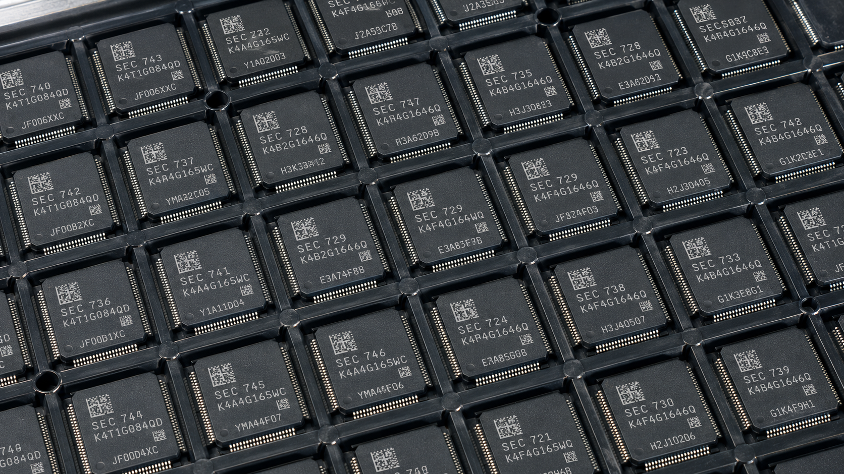
The semiconductor and precision electronics industry represents the forefront of global manufacturing technology. As IC chips continue to shrink in size while increasing in complexity and functionality, the demands on marking technology have never been greater. Precision components — including IC chips, memory modules, MEMS sensors, power semiconductors, and passive SMD components — must carry permanent, high-density identification codes within microscopic areas, all while maintaining absolute device integrity and zero defects.
Key drivers shaping the industry include:
- Global Market Expansion:
The worldwide semiconductor market continues to grow rapidly, with increasing demand for traceability across the entire supply chain — from wafer fabrication to final assembly.
- Stringent Industry Standards:
Quality standards such as IPC-A-610 and JEDEC specifications require marking to remain readable through multiple process steps and harsh environmental conditions (reflow soldering, thermal cycling, cleaning processes).
- Miniaturization Pressure:
As package sizes shrink to 0201, 01005, and even smaller, traditional marking technologies (inkjet, labeling, dot peen) have reached their physical limitations in terms of precision and reliability.
UV ultraviolet lasers have emerged as the industry-standard solution for marking IC chips and precision components, delivering the required precision, speed, and zero-damage performance demanded by this exacting sector.
II. Core Challenges
1. Micro-Scale Marking Area:
IC chips and ultra-miniature components (0201, 01005 packages, and CSP/WLCSP devices) require marking precision at the micron or even sub-micron level, with feature sizes down to a few micrometers.
2. Zero Thermal Damage Requirement:
Semiconductor materials (silicon, gallium arsenide, silicon carbide) and delicate PCB substrates are extremely heat-sensitive. Any thermal impact during marking can alter electrical characteristics, create micro-cracks, or compromise device reliability.
3. High-Density Data Encoding:
Advanced traceability requires 2D codes (DataMatrix, QR) carrying extensive information (lot numbers, wafer IDs, X/Y coordinates, testing data) to be laser-engraved within areas as small as 1mm x 1mm.
4. Electrostatic Discharge (ESD) Protection:
CMOS-based chips, gate arrays, and other electrostatic-sensitive devices can be destroyed by static electricity generated during conventional marking processes. ESD-safe marking solutions are essential.
5. Full-Lifecycle Traceability:
Complete traceability is required from wafer sort, through assembly and test, to final system integration. Marks must remain legible across multiple thermal cycles, cleaning processes, and handling steps.
6. Zero Defect Tolerance:
Marking processes must generate no particulates, micro-cracks, burrs, or surface contamination that could interfere with subsequent photolithography, wire bonding, or underfill processes.
III. Laser Solution: UV Laser — The Gold Standard for IC and Precision Component Marking
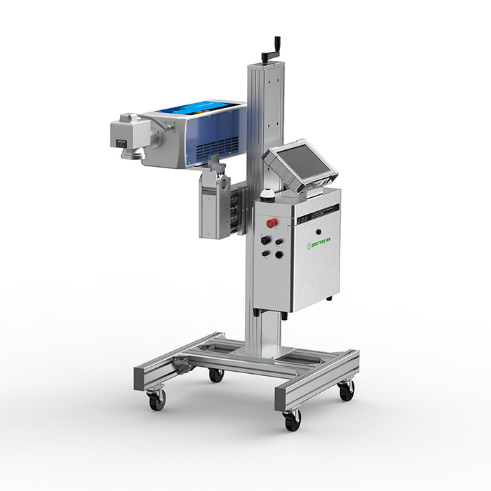
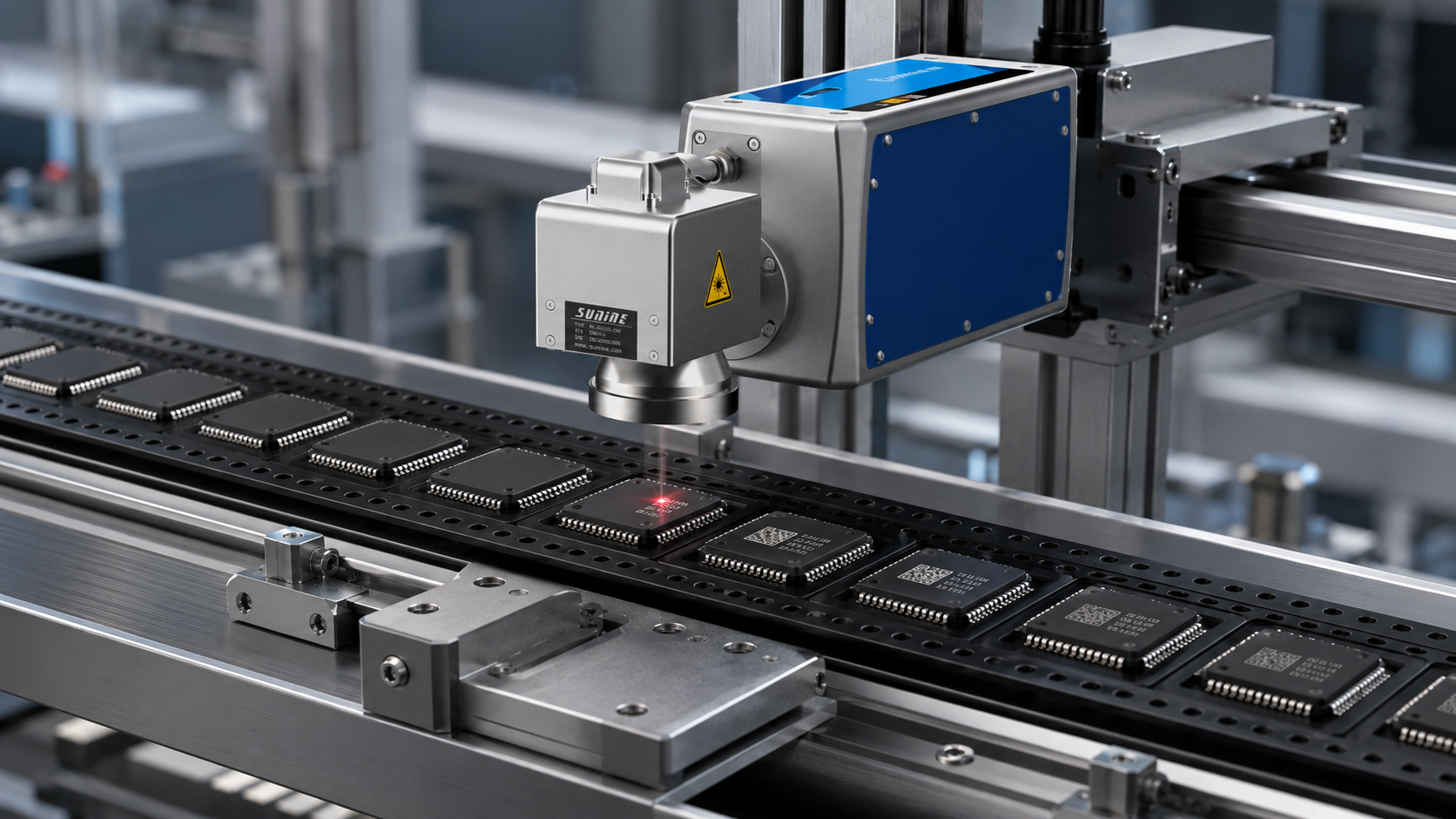
UV ultraviolet lasers (355nm wavelength) deliver extremely short pulses with high peak power, enabling material removal through photochemical ablation (cold ablation) rather than thermal effects. This "cold marking" mechanism ensures virtually zero heat-affected zone (HAZ), preserving the structural and electrical integrity of sensitive semiconductor devices.
Why UV Laser for IC Chips and Precision Components:
- Cold Processing: Minimal thermal stress, no micro-cracks, no delamination, no alteration of electrical properties.
- Sub-Micron Precision: Capable of producing feature sizes well below 1 micron, suitable for the smallest component packages.
- Versatile Material Compatibility: Works on a wide range of materials including silicon, silicon carbide, gallium arsenide, ceramic substrates, glass, organic laminates, and passivation layers.
- High-Contrast Marks: Produces clear, readable codes that withstand harsh downstream processes (reflow soldering up to 260C, thermal cycling, cleaning).
- ESD-Safe Operation: Designed with anti-static measures to protect sensitive devices.
- High Throughput: Supports high-volume production with fast marking speeds, seamlessly integrating with automated pick-and-place and test-handling equipment.
Technical Specifications:
Laser Type: UV ultraviolet laser (355nm wavelength)
Marking Mechanism: Photochemical ablation (cold marking), non-thermal
Heat-Affected Zone: Negligible (typically < 10 micrometers)
Marking Precision: Sub-micron level (< 1 micrometer)
Applicable Materials: Silicon, SiC, GaAs, ceramic substrates, PCB laminates, glass, passivation films
Marking Content: DataMatrix codes, QR codes, batch/lot numbers, wafer IDs, coordinate data, serial numbers
ESD Protection: Built-in anti-static design for safe handling of CMOS and other ESD-sensitive devices
IV. Typical Applications
- IC Packages: Marking on leadframes, plastic packages, ceramic packages, and CSP/WLCSP devices
- Passive Components: Laser coding on resistors, capacitors, inductors (0201/01005 sizes)
- MEMS Devices: Micro-machined sensors requiring precision marking without damaging delicate structures
- Power Semiconductors: Marking on IGBTs, MOSFETs, and silicon carbide devices
- Connectors and Contacts: Permanent identification on precision pins and terminals
- Wafer-Level Marking: Die traceability marks applied at wafer sort stage